Update2026.06.06 (토)


[Huawei's Grandiose Promotion of a "New Law of Semiconductors"...]
Huawei has proclaimed the "Tau (τ) Law" to replace Moore's Law—the 60-year-old guiding principle of the semiconductor industry. However, the company's own technical paper is filled with exaggerated claims and theories that fail to overcome practical limitations, drawing harsh criticism from experts. Most notably, Huawei has subtly hinted at its own defeat, acknowledging that it cannot break through the Extreme Ultraviolet (EUV) lithography barrier.
On June 5, The Wall Street Journal (WSJ) reported:
"At the IEEE International Symposium on Circuits and Systems (ISCAS 2026) held in Shanghai on May 25, He Tingbo, a member of Huawei's board of directors and president of its semiconductor division, officially announced the Tau (τ) scaling law during a keynote speech titled 'Exploration and Practice of New Semiconductor Pathways.' This law proposes shifting the benchmark of semiconductor advancement from 'geometric scaling' via the physical shrinking of transistors to 'temporal scaling,' which compresses signal transmission time (τ). Huawei claimed this law would become a new principle guiding the overall development of semiconductors and electronic systems."
The People's Daily, the official mouthpiece of the Chinese Communist Party, heavily promoted the announcement, declaring that "a Chinese company has, for the first time, presented a developmental principle for the global semiconductor industry." The publication added:
"He Tingbo revealed that Huawei has designed and mass-produced 381 chips based on the Tau Law over the past six years. She also announced that the new Kirin smartphone processor, scheduled for release in the fall of 2026, will feature the 'LogicFolding' architecture for the first time. Huawei stated it aims to increase transistor density by 55% and achieve 1.4-nanometer-class performance by 2031. Following this news, shares of SMIC, China's largest foundry, surged by over 19% the next day."
In response, major South Korean media outlets immediately ran grandiose headlines such as, "U.S. Pressure Backfires, Triggering Chinese Innovation... Huawei Snapping at TSMC's Heels," claiming that American pressure had created a "butterfly effect" that catalyzed China's independent technological advancements.
[The Truth Exposed by Huawei's Own Technical Paper]
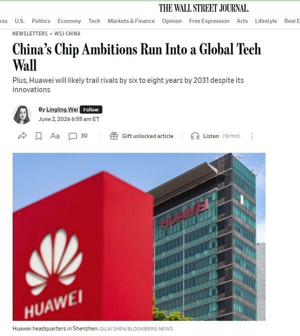
However, experts who meticulously reviewed the original text of Huawei's technical paper offer a bleak assessment. Lingling Wei, the Chief China Correspondent for the WSJ, pointed out in an analysis piece dated June 2 that "the paper contains content completely contrary to Huawei's public narrative."
According to Wei, the paper explicitly states in its introduction: "For companies restricted from accessing the most advanced lithography equipment, those constraints apply sooner and more severely." It goes on to note, "The assumption that another process node will solve the problem is no longer valid." Wei highlighted that "this is effectively an official declaration in a formal document that Huawei has abandoned attempts to bypass the EUV barrier."
The WSJ further noted:
"Jimmy Goodrich, an independent semiconductor analyst who reviewed this paper, is a senior fellow at the UC Irvine Institute on Global Conflict and Cooperation (IGCC), an advisor to the RAND Corporation, and a leading authority who served as vice president of the Semiconductor Industry Association (SIA) for nearly a decade. He bluntly stated, 'The engineering achievement itself is impressive, but the framing of it as a breakthrough is not. Huawei is working cleverly with the tools available to them—that is the real story.' He added that the paper is the clearest statement yet from within Huawei admitting that the EUV barrier cannot be breached anytime soon."
["Stacking" is Not a New Technology]
The methodology Huawei adopted to boost semiconductor performance without EUV is a 3D stacking technology dubbed "LogicFolding." This principle improves performance by vertically stacking two circuit layers instead of using a traditional single-layer circuit structure, thereby shortening the distance signals must travel.
While South Korean media highly praised this aspect, the problem is that this is not an exclusive Huawei invention. TSMC, Intel, AMD, and Samsung are already utilizing stacking technology extensively. The critical difference is that their stacking designs are implemented on advanced chips manufactured using EUV lithography. In other words, while competitors combine advanced nodes with stacking technology, Huawei plans to bridge the gap using stacking alone, without advanced nodes. This can be viewed as little more than a clever optical illusion rather than a genuine technological breakthrough.
Jimmy Goodrich, who is also a senior fellow at the Center for Strategic and International Studies (CSIS), quantified this gap clearly:
"TSMC is scheduled to achieve the performance level in 2028 that Huawei aims to reach only by 2031. By 2031, TSMC will have taken another leap forward by applying the same stacking technology to much more advanced nodes. The realistic gap in 2031 is expected to be around 6 to 8 years."
This presents a completely different reality from the 3-year gap implied by Huawei's announcement.
[The 20% Yield Trap: Viable for Prototypes, Impossible for Commercialization]
The issues do not end there. The WSJ pointed out that "the technical fiction goes beyond this," noting that Goodrich estimated Huawei's actual mass-production yield to be around 20%. This means that out of every five chips manufactured, four are discarded as defective.
The WSJ noted:
"Stacking technology requires bonding two chips together with extreme precision. When it is already difficult to manufacture a single chip properly, the yield for stacking—which requires making two perfect chips simultaneously and bonding them flawlessly—is bound to drop exponentially."
Dr. Ian Cutress, a semiconductor expert, also pointed out that "the hybrid bonding method consumes about 10 times more energy per unit area compared to producing cutting-edge EUV 2nm transistors." Higher energy consumption slows production speeds and makes securing a viable yield of defect-free products even more difficult.
Global Semi Research also analyzed that this is a "multi-year process development challenge requiring the miniaturization of TSV (Through-Silicon Via) diameters and pitches, achieving an alignment precision within 0.5 micrometers, and approaching a 100% yield through intelligent redundant design."
Miniaturization of TSV Diameter and Pitch: This means the vertical pathways (TSVs, copper pillars much thinner than a human hair) that electrically connect two chips must be packed more densely. If the pillars are thick or widely spaced, data moves slowly, defeating the purpose of stacking.
0.5-Micrometer Alignment Precision: The circuits of the top and bottom chips must be aligned precisely within a margin of error of 0.5 micrometers (about 1/150th the width of a human hair). Even a slight misalignment causes broken circuits or malfunctions.
Approaching 100% Yield: Currently, four out of five individual chips made by Huawei are defective. To bond two chips, both must be defect-free simultaneously, and no defects can occur during the bonding process itself. If there is even a minor defect rate, the final yield plummets drastically.
In conclusion, the phrase "a multi-year process development challenge" indicates that this technology is currently only viable at a laboratory level, and it will take several more years to mass-produce it stably in a factory setting. While the technology announced by Huawei is not inherently false, this serves as the basis for criticism that it remains far from mass production and commercialization.
[A Simultaneous Political Signal to Both the U.S. and China]
Experts analyze that the true purpose of this announcement is not a display of technological prowess, but rather the delivery of a political message. Huawei's announcement targets two entirely different audiences simultaneously.
To Washington, it signals that "export controls are not working," providing political leverage to factions advocating for the relaxation of regulations. To Beijing, it provides a narrative that renders the high-performance Nvidia chip licenses—which President Trump recently approved but China has not yet purchased—unnecessary. This feeds into the self-reliance narrative: "We have forged our own path without American technology."
However, Goodrich offered a sobering assessment, stating, "Export controls are working—they just have a lot of loopholes." In fact, the U.S. Department of Commerce's Bureau of Industry and Security (BIS) explicitly stated in a guidance released on May 31:
"Export control licensing requirements for entities headquartered in China apply equally to proxy transactions conducted via overseas subsidiaries."
This directive clarifies that the application of export controls is based on corporate ownership and headquarters location rather than the physical location of a subsidiary. This measure effectively acknowledges and blocks the practice of Chinese-headquartered companies purchasing advanced chips through overseas corporate entities.
[Excessive Pro-China Distortions in South Korean Media Coverage]
Certain segments of the domestic media are linking Huawei's announcement of the Tau Law with the rise of Chinese AI, such as DeepSeek, creating an exaggerated narrative of a "monster born of the U.S. blockade." However, this is a narrative refuted by Huawei's paper itself. Huawei did not break through the EUV barrier; rather, it internally acknowledged its inability to do so and shifted to a strategy of moving as cleverly as possible within those constraints.
In her WSJ analysis, Lingling Wei evaluated that "Huawei's announcement of the Tau Law is paradoxically evidence that export controls are proving effective." She added, "The confident proclamations felt at Huawei's R&D campus in 2019 now read as an announcement packaged to conceal limitations."
What experts are focusing on is not the claim that Huawei has opened a new era of semiconductors, but rather the fact that it has effectively chosen a strategic retreat from the existing competitive landscape.
The Tau Law and LogicFolding are not declarations that Huawei will overtake TSMC without EUV. Instead, they are closer to a survival strategy aimed at maximizing performance improvements under highly restricted conditions, having accepted the reality that EUV cannot be acquired.
Therefore, interpreting this announcement as a declaration of victory for Chinese semiconductors is an extreme leap of logic. Huawei has not presented a new path; rather, it has revealed that its options have been severely limited by U.S. export controls, forcing it to seek detours.
Ultimately, what this Tau Law announcement demonstrates is not a 'technological breakthrough by China,' but the persistent existence of the unbreached EUV barrier. What Huawei truly needs to prove is not the theories in its paper, but the much harsher realities of yield, productivity, and large-scale commercialization.

-중국 푸단대학교 한국연구원 객좌교수
-전 EDUIN News 대표
-전 OUR NEWS 대표
-제17대 대통령직인수위원회 정책기획팀장
-전 대통령실 홍보기획비서관
-사단법인 한국가정상담연구소 이사장
-저서: 북한급변사태와 한반도통일, 2012 다시우파다, 선거마케팅, 한국의 정치광고, 국회의원 선거매뉴얼 등 50여권